| CPC H01L 21/845 (2013.01) [H01L 29/0673 (2013.01); H01L 29/42392 (2013.01); H01L 29/78391 (2014.09); H01L 29/7853 (2013.01); H10B 51/10 (2023.02); H10B 51/30 (2023.02)] | 20 Claims |
|
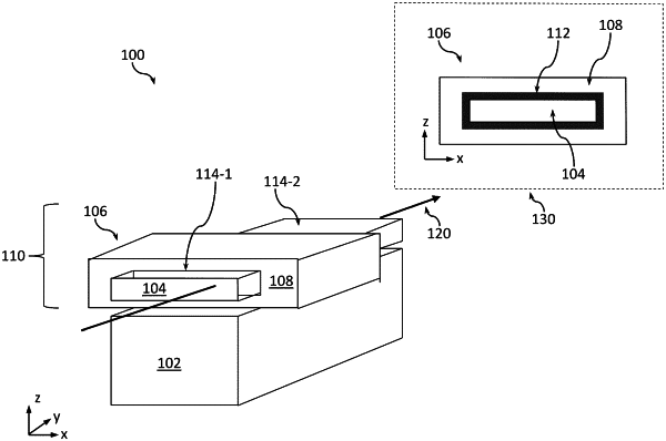
1. A transistor arrangement, comprising:
a substrate;
a base comprising a face that is opposite the substrate, a first sidewall between the face and the substrate, and a second sidewall opposite the first sidewall;
a nanoribbon comprising a first semiconductor material and having a longitudinal axis substantially parallel to the substrate, where the base is between the substrate and the nanoribbon;
a gate insulator-wrapping around a portion of the nanoribbon between a first plane and a second plane, where each of the first plane and the second plane is substantially perpendicular to the longitudinal axis of the nanoribbon; and
an opening partially filled with a first insulator and partially filled with a second insulator, the opening extending in a direction substantially parallel to the longitudinal axis of the nanoribbon, wherein the second insulator is closer to the substrate than the first insulator and is etch selective with respect to the first insulator.
|