| CPC H01L 21/823481 (2013.01) [H01L 21/761 (2013.01); H01L 21/823475 (2013.01); H01L 24/80 (2013.01); H01L 2224/80895 (2013.01); H01L 2224/80896 (2013.01)] | 2 Claims |
|
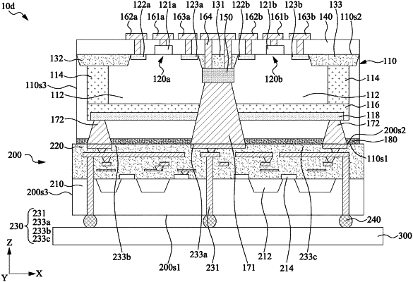
1. A method of manufacturing a semiconductor device structure, comprising:
providing a substrate having a first surface and a second surface opposite to the first surface, wherein the substrate comprises a first well region with a first conductive type;
forming an isolation feature extending from the second surface of the substrate;
forming a first transistor and a second transistor adjacent to the second surface of the substrate;
forming a first doped region under the isolation feature, wherein the first doped region has a second conductive type different from the first conductive type;
providing a circuit structure on the first surface of the substrate, wherein the circuit structure is configured to transmit or provide a voltage electrically coupled with the first doped region;
forming a first conductive feature extending between the first surface of the substrate and the first doped region, wherein the first conductive feature electrically couples with the circuit structure;
forming a second well region in the substrate and surrounding the first doped region; and
forming a third well region spaced apart from the second surface of the substrate and in contact with the second well region.
|