| CPC H01L 21/823481 (2013.01) [H01L 21/0259 (2013.01); H01L 21/823412 (2013.01); H01L 21/823431 (2013.01); H01L 27/0886 (2013.01); H01L 29/0642 (2013.01); H01L 29/0665 (2013.01); H01L 29/42392 (2013.01); H01L 29/66545 (2013.01); H01L 29/66742 (2013.01); H01L 29/66795 (2013.01); H01L 29/7851 (2013.01); H01L 29/78696 (2013.01)] | 10 Claims |
|
6. A preparation method of an integrated circuit device, comprising:
forming, on the substrate, a fin protruding from a substrate;
forming at least two first dummy gates and at least one second dummy gate, wherein the at least two first dummy gates and the at least one second dummy gate are arranged in a gate length direction, each second dummy gate is located between two adjacent first dummy gates, and the first dummy gates and the second dummy gate all are in contact with two opposite side surfaces and a top surface of the fin;
forming an inter-layer insulating layer, wherein an upper surface of the inter-layer insulating layer is aligned with upper surfaces of the second dummy gate and the first dummy gates;
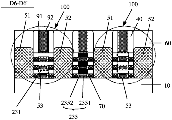
removing at least the second dummy gate, and processing a part that is of the fin and that is exposed after the second dummy gate is removed, to form an isolation section as a portion of a first semiconductor layer in the part that is of the fin, and wherein the part of the fin processed to form the isolation section further suppresses current transfer in the part that is of the fin and that is exposed after the second dummy gate is removed, wherein the isolation section comprises discontinuity in the first semiconductor layer within the part that is of the fin; and
forming an auxiliary layer that alternates with the isolation section and the channels in respective regions in the fin, wherein the auxiliary layer comprises a gate material layer and a gate dielectric material layer that is wrapped outside the gate material layer.
|