US 12,068,201 B2
Semiconductor devices
Shih-Chieh Wu, Hsinchu (TW); Pang-Chi Wu, Hsinchu (TW); Kuo-Yi Chao, Hsinchu (TW); Mei-Yun Wang, Chu-Pei (TW); Hsien-Huang Liao, Hsinchu (TW); Tung-Heng Hsieh, Zhudong Town (TW); and Bao-Ru Young, Zhubei (TW)
Assigned to TAIWAN SEMICONDUCTOR MANUFACTURING COMPANY, LTD., Hsinchu (TW)
Filed by Taiwan Semiconductor Manufacturing Co., Ltd., Hsinchu (TW)
Filed on Jun. 15, 2023, as Appl. No. 18/335,806.
Application 18/335,806 is a continuation of application No. 17/862,628, filed on Jul. 12, 2022, granted, now 11,721,590.
Application 17/862,628 is a continuation of application No. 17/169,809, filed on Feb. 8, 2021, granted, now 11,393,724, issued on Jul. 19, 2022.
Application 17/169,809 is a continuation of application No. 16/567,053, filed on Sep. 11, 2019, granted, now 10,957,604, issued on Mar. 23, 2021.
Claims priority of provisional application 62/753,456, filed on Oct. 31, 2018.
Prior Publication US 2023/0326804 A1, Oct. 12, 2023
Int. Cl. H01L 21/82 (2006.01); H01L 21/76 (2006.01); H01L 21/768 (2006.01); H01L 21/8234 (2006.01); H01L 29/66 (2006.01)
CPC H01L 21/823475 (2013.01) [H01L 21/76805 (2013.01); H01L 21/7682 (2013.01); H01L 21/76895 (2013.01); H01L 21/823431 (2013.01); H01L 21/823437 (2013.01); H01L 29/66545 (2013.01)] 20 Claims
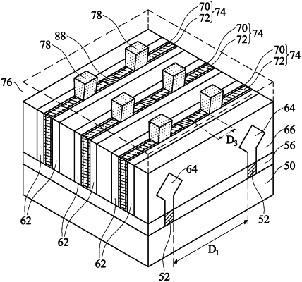
OG exemplary drawing
 
1. A device comprising:
a first metal gate stack over a substrate;
a second metal gate stack over the substrate;
a dielectric material between a first end of the first metal gate stack and a second end of the second metal gate stack;
an inter-layer dielectric over the dielectric material, the first metal gate stack, and the second metal gate stack;
a first gate contact extending through the inter-layer dielectric to physically contacting the first metal gate stack; and
a second gate contact extending through the inter-layer dielectric to physically contacting the second metal gate stack, wherein half of a distance between the first gate contact and the second gate contact is larger than a distance between the first gate contact and the dielectric material and is larger than a distance between the second gate contact and the dielectric material.