| CPC H01L 21/823412 (2013.01) [H01L 21/2253 (2013.01); H01L 21/28185 (2013.01); H01L 29/6675 (2013.01); H01L 27/088 (2013.01); H01L 29/7869 (2013.01); H01L 29/78696 (2013.01)] | 6 Claims |

|
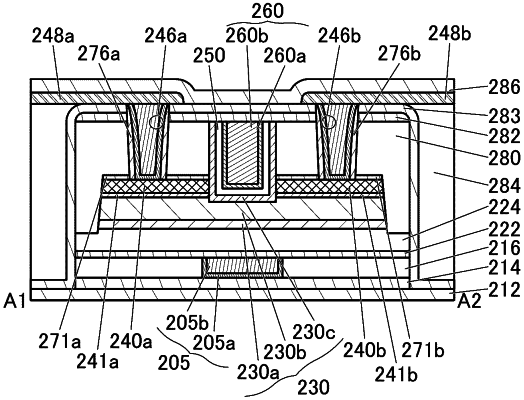
1. A method for manufacturing a semiconductor device, comprising:
forming a first insulator;
forming an island-shaped stacked body in which a first oxide, a second oxide, and a first conductor are stacked in this order over the first insulator;
forming a second insulator over the first insulator and the stacked body;
forming an opening portion for exposing the stacked body in the second insulator;
exposing a top surface of the second oxide by removing a region of the first conductor exposed in the opening portion, forming a second conductor and a third conductor over the second oxide, and then performing cleaning treatment;
forming a first oxide film in contact with a side surface of the first oxide and top and side surfaces of the second oxide that are exposed in the opening portion;
performing oxygen addition treatment on a vicinity of an interface between the second oxide and the first oxide film through the first oxide film and then performing heat treatment; and
forming a first insulating film and a first conductive film over the first oxide film, and then removing parts of the first conductive film, the first insulating film, the first oxide film, and the second insulator by chemical polishing treatment to expose the second insulator and form a fourth conductor, a third insulator, and a third oxide in the opening portion provided in the second insulator.
|