| CPC H01L 21/76895 (2013.01) [H01L 21/2885 (2013.01); H01L 21/76829 (2013.01); H01L 21/76831 (2013.01); H01L 21/7684 (2013.01); H01L 21/76849 (2013.01); H01L 21/76874 (2013.01); H01L 21/76877 (2013.01); H01L 21/76879 (2013.01); H01L 21/76883 (2013.01); H01L 29/41775 (2013.01); H01L 29/66477 (2013.01); H01L 29/665 (2013.01); H01L 29/66553 (2013.01); H01L 29/78 (2013.01); H01L 29/7833 (2013.01); H01L 21/28518 (2013.01); H01L 21/76843 (2013.01); H01L 21/76855 (2013.01); H01L 21/76873 (2013.01); H01L 23/485 (2013.01)] | 20 Claims |
|
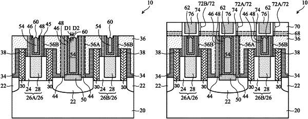
1. An integrated circuit comprising:
a semiconductor region;
a gate stack over the semiconductor region;
a source/drain region in the semiconductor region;
a contact plug over and electrically coupling to the gate stack or the source/drain region, the contact plug comprising:
a metal feature; and
a first layer comprising sidewall portions on opposite sides of the metal feature, and a bottom portion overlapped by the metal feature; and
a conductive layer comprising:
a middle portion overlapping and contacting the metal feature; and
an end portion on a side of the middle portion, wherein the end portion is thicker than the middle portion, wherein the end portion that is thicker than the middle portion also overlaps an inner portion of one of the sidewall portions of the first layer, and wherein a curved interface is formed between the end portion and the metal feature.
|