US 12,068,194 B2
Selective deposition of metal barrier in damascene processes
Chia-Pang Kuo, Taoyuan (TW); Ya-Lien Lee, Baoshan Township (TW); and Chieh-Yi Shen, Taipei (TW)
Assigned to TAIWAN SEMICONDUCTOR MANUFACTURING COMPANY, LTD., Hsinchu (TW)
Filed by Taiwan Semiconductor Manufacturing Co., Ltd., Hsinchu (TW)
Filed on Aug. 2, 2023, as Appl. No. 18/364,286.
Application 17/809,919 is a division of application No. 16/213,622, filed on Dec. 7, 2018, granted, now 11,398,406, issued on Jul. 26, 2022.
Application 18/364,286 is a continuation of application No. 17/809,919, filed on Jun. 30, 2022, granted, now 11,837,500.
Claims priority of provisional application 62/738,414, filed on Sep. 28, 2018.
Prior Publication US 2024/0006234 A1, Jan. 4, 2024
Int. Cl. H01L 21/768 (2006.01); H01L 23/522 (2006.01); H01L 23/532 (2006.01)
CPC H01L 21/76844 (2013.01) [H01L 21/7681 (2013.01); H01L 21/76879 (2013.01); H01L 23/5226 (2013.01); H01L 23/53238 (2013.01)] 20 Claims
OG exemplary drawing
 
1. A method comprising:
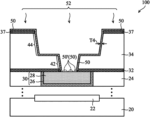
forming an etch stop layer over a conductive feature;
forming a dielectric layer over the etch stop layer;
forming an opening in the dielectric layer and the etch stop layer to reveal the conductive feature;
selectively depositing an inhibitor film comprising an inhibitor on the conductive feature;
selectively depositing a conductive barrier layer extending into the opening and on exposed surfaces of the dielectric layer;
after the conductive barrier layer is selectively deposited, removing the inhibitor film; and
depositing a conductive material to fill a remaining portion of the opening.