| CPC H01L 21/6835 (2013.01) [G11C 8/16 (2013.01); H01L 21/743 (2013.01); H01L 21/76254 (2013.01); H01L 21/76898 (2013.01); H01L 21/8221 (2013.01); H01L 21/823828 (2013.01); H01L 21/84 (2013.01); H01L 23/481 (2013.01); H01L 23/5252 (2013.01); H01L 27/0207 (2013.01); H01L 27/0688 (2013.01); H01L 27/092 (2013.01); H01L 27/10 (2013.01); H01L 27/105 (2013.01); H01L 27/11807 (2013.01); H01L 27/11898 (2013.01); H01L 27/1203 (2013.01); H01L 29/4236 (2013.01); H01L 29/66272 (2013.01); H01L 29/66621 (2013.01); H01L 29/66825 (2013.01); H01L 29/66833 (2013.01); H01L 29/66901 (2013.01); H01L 29/78 (2013.01); H01L 29/7841 (2013.01); H01L 29/7843 (2013.01); H01L 29/7881 (2013.01); H01L 29/792 (2013.01); H10B 10/00 (2023.02); H10B 10/125 (2023.02); H10B 12/053 (2023.02); H10B 12/09 (2023.02); H10B 12/20 (2023.02); H10B 12/50 (2023.02); H10B 20/00 (2023.02); H10B 41/20 (2023.02); H10B 41/40 (2023.02); H10B 41/41 (2023.02); H10B 43/20 (2023.02); H10B 43/40 (2023.02); H01L 23/3677 (2013.01); H01L 24/13 (2013.01); H01L 24/16 (2013.01); H01L 24/45 (2013.01); H01L 24/48 (2013.01); H01L 25/0655 (2013.01); H01L 25/0657 (2013.01); H01L 25/50 (2013.01); H01L 27/1214 (2013.01); H01L 27/1266 (2013.01); H01L 2221/68368 (2013.01); H01L 2223/5442 (2013.01); H01L 2223/54426 (2013.01); H01L 2224/131 (2013.01); H01L 2224/16145 (2013.01); H01L 2224/16146 (2013.01); H01L 2224/16227 (2013.01); H01L 2224/16235 (2013.01); H01L 2224/32145 (2013.01); H01L 2224/32225 (2013.01); H01L 2224/45124 (2013.01); H01L 2224/45147 (2013.01); H01L 2224/48091 (2013.01); H01L 2224/48227 (2013.01); H01L 2224/73204 (2013.01); H01L 2224/73253 (2013.01); H01L 2224/73265 (2013.01); H01L 2224/81005 (2013.01); H01L 2224/83894 (2013.01); H01L 2225/06513 (2013.01); H01L 2225/06541 (2013.01); H01L 2924/00011 (2013.01); H01L 2924/01002 (2013.01); H01L 2924/01004 (2013.01); H01L 2924/01013 (2013.01); H01L 2924/01018 (2013.01); H01L 2924/01019 (2013.01); H01L 2924/01029 (2013.01); H01L 2924/01046 (2013.01); H01L 2924/01066 (2013.01); H01L 2924/01068 (2013.01); H01L 2924/01077 (2013.01); H01L 2924/01078 (2013.01); H01L 2924/01322 (2013.01); H01L 2924/10253 (2013.01); H01L 2924/10329 (2013.01); H01L 2924/12032 (2013.01); H01L 2924/12033 (2013.01); H01L 2924/12036 (2013.01); H01L 2924/12042 (2013.01); H01L 2924/1301 (2013.01); H01L 2924/1305 (2013.01); H01L 2924/13062 (2013.01); H01L 2924/13091 (2013.01); H01L 2924/14 (2013.01); H01L 2924/1461 (2013.01); H01L 2924/15311 (2013.01); H01L 2924/1579 (2013.01); H01L 2924/16152 (2013.01); H01L 2924/181 (2013.01); H01L 2924/19041 (2013.01); H01L 2924/30105 (2013.01); H01L 2924/3011 (2013.01); H01L 2924/3025 (2013.01); H10B 12/05 (2023.02); H10B 20/20 (2023.02)] | 20 Claims |
|
1. A 3D semiconductor device, the device comprising:
a first level comprising a first single crystal layer, said first level comprising first transistors,
wherein each of said first transistors comprises a single crystal channel;
first metal layer;
a second metal layer overlaying said first metal layer; and
a second level comprising a second single crystal layer, said second level comprising second transistors and at least one third metal layer,
wherein said second level overlays said first level,
wherein at least one of said second transistors comprises a transistor channel,
wherein said second level comprises a plurality of DRAM memory cells,
wherein each of said plurality of DRAM memory cells comprises at least one of said second transistors and one capacitor,
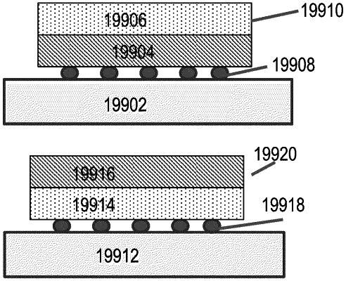
wherein said second level is directly bonded to said first level, and
wherein said bonded comprises metal to metal bonds.
|