| CPC H01L 21/67121 (2013.01) [B65G 51/02 (2013.01); H01L 21/67333 (2013.01)] | 24 Claims |
|
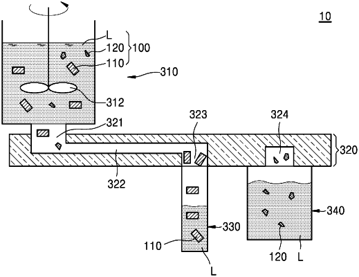
1. A chip transfer apparatus configured to align a plurality of micro-semiconductor chips in a plurality of grooves of a transfer substrate, the chip transfer apparatus comprising:
a chip storage module configured to store a suspension including the plurality of micro-semiconductor chips and impurities;
a chip filtration module configured to receive the suspension from the chip storage module and separate a first suspension including the plurality of micro-semiconductor chips and a second suspension including the impurities; and
a chip supply module configured to supply the first suspension onto the transfer substrate from the chip filtration module, wherein the plurality of micro-semiconductor chips included in the first suspension are flowable on the transfer substrate,
wherein the chip filtration module comprises:
an inlet connected to a lower area of the chip storage module, the inlet configured to receive the suspension introduced from the chip storage module;
a channel connected to the inlet and through which the suspension flows; and
a first outlet connected to the channel and an upper area of the chip supply module and configured to discharge the first suspension to the chip supply module.
|