| CPC H01L 21/67098 (2013.01) [H01L 24/11 (2013.01); H01L 24/13 (2013.01)] | 18 Claims |
|
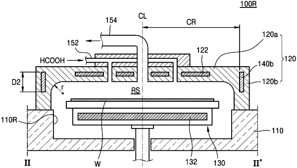
1. A method of manufacturing a solder bump, the method comprising:
providing a substrate, comprising a solder bump which is not reflowed, to a supporter in a reflow space defined by a housing and a cover;
applying energy to an edge heating zone provided along a perimeter of the cover;
supplying an oxide remover to the substrate; and
heating a supporter heating part provided in the supporter, for reflowing the solder bump,
wherein the cover comprises a first portion substantially parallel to a main surface of the substrate and a second portion substantially vertical to the main surface of the substrate, and
the edge heating zone is provided in the first portion of the cover.
|