| CPC H01L 21/4882 (2013.01) [H01L 21/4842 (2013.01); H01L 23/3672 (2013.01); H01L 23/3677 (2013.01); H01L 23/473 (2013.01); H01L 2924/0002 (2013.01); H05K 7/20927 (2013.01)] | 23 Claims |

|
1. A method comprising:
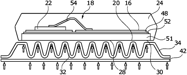
providing a power semiconductor module that comprises a substrate having a first substrate side for carrying at least one electric circuit and having a second substrate side being located opposite to the first substrate side, wherein the second substrate side has a flat surface, and wherein located at the second substrate side is a cooling area that is surrounded by a connecting area;
connecting a first casing component of a cooler to the second substrate side at the connecting area,
connecting a second casing component to the first casing component such that a cooling channel for providing the cooling area with cooling fluid is provided between the first casing component and the second casing component; and
welding a cooling structure to the cooling area at the second substrate side, the cooling structure having a wavy form.
|