| CPC H01L 21/3085 (2013.01) [H01L 21/3088 (2013.01); H01L 21/31144 (2013.01); H01L 21/76802 (2013.01); H01L 21/76898 (2013.01)] | 20 Claims |
|
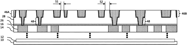
1. A method comprising:
patterning a first patterning layer over a target layer to form a first pattern and a second pattern;
depositing a spacer structure over the first pattern and the second pattern;
masking a first portion of the spacer structure overlying the first pattern, a second portion of the spacer structure exposed from the mask;
etching the second portion of the spacer structure to at least thin the second portion of the spacer structure;
unmasking the first portion of the spacer structure;
forming a spacer mask, wherein forming the spacer mask comprises anisotropically etching the first portion of the spacer structure;
removing the first pattern, leaving behind the spacer mask; and
etching the target layer based on the spacer mask.
|