| CPC H01L 21/28556 (2013.01) [H01L 21/02274 (2013.01); H01L 21/28568 (2013.01); H01L 21/3212 (2013.01); H01L 21/477 (2013.01); H01L 21/823431 (2013.01)] | 19 Claims |
|
1. A method for forming a semiconductor structure, comprising:
providing a substrate;
forming a gate electrode layer on the substrate;
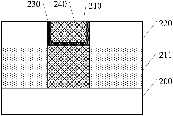
forming an interlayer dielectric layer on top surfaces of the gate electrode layer and the substrate;
forming a contact opening in the interlayer dielectric layer to expose the top surface of the gate electrode layer;
performing a defluorination treatment on the gate electrode layer; and
after performing the defluorination treatment, forming a barrier material film in the contact opening and on a top surface of the interlayer dielectric layer, and planarizing the barrier material film until the top surface of the interlayer dielectric layer is exposed, to form a barrier layer in the contact opening and on the top surface of the gate electrode layer, wherein the barrier layer is made of a material including titanium element, and a top surface of the barrier layer is coplanar with the top surface of the interlayer dielectric layer.
|