| CPC H01L 21/26553 (2013.01) [H01L 29/04 (2013.01); H01L 29/66204 (2013.01)] | 9 Claims |

|
1. A method of forming a semiconductor device on a gallium and nitrogen containing material, the method comprising:
providing a substrate member comprising a surface region, the substrate member comprising a gallium and nitrogen bearing material, the surface region being configured along a c-plane having an off-set cut along a direction of an m-plane;
forming a thickness of epitaxial material comprising a gallium and nitrogen bearing material, using a MOCVD or HVPE process overlying the surface region, the thickness of epitaxial material having an upper surface region, the epitaxial material having a silicon dopant concentration of 1E15 to 5E16 atoms/centimeter cubed, and the thickness ranging from 1 micron to 3 micron or 50 microns to 60 microns, and a surface roughness;
subjecting the upper surface region of the thickness of epitaxial material to a cleaning solution using a combination of a solvent mixture and an acid containing mixture;
subjecting the upper surface region to a plurality of particles to implant the plurality of particles through the upper surface region to a depth as measured from the upper surface region such that the plurality of particles forms the implant profile within the depth and having a peak within a region below the upper surface of the thickness of epitaxial material such that the implant causes crystalline damage to a portion of the epitaxial material to cause the epitaxial material to become amorphous in state;
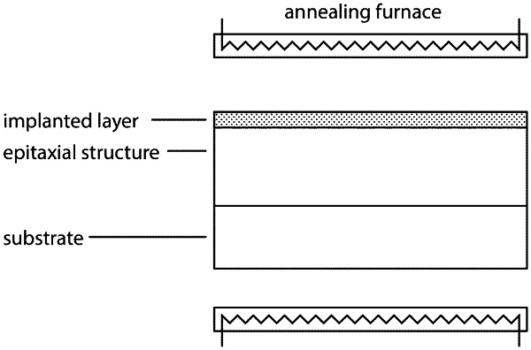
subjecting the substrate member, the epitaxial material, and an implant profile to a thermal energy to anneal the epitaxial material including the implant profile at a temperature of 700 to 1500° C. using an ammonia containing environment for a time period of 1 to 3000 seconds to cause a hydrogen containing environment to create atomic hydrogen to interact with the plurality of particles; and thereafter removing the hydrogen containing environment using a nitrogen containing environment to drive out hydrogen species from the epitaxial material including the implant profile thereby removing a crystalline damage from the epitaxial material to change the amorphous state to a single crystalline state, and thereby creating an electrically activated crystalline material and form a p-n junction between the implant profile and a remainder of the epitaxial material; and
subjecting the upper surface region to an etching process, the etching process is a dry etching process or a wet etching process, to adjust a characteristic of the upper surface region from a first state to a second state, the first state comprises a first current value and a second state comprises a second current value, whereby the second current value is greater than the first current value.
|