| CPC H01L 21/0337 (2013.01) [H01L 28/60 (2013.01); H01L 21/0332 (2013.01); H01L 21/31144 (2013.01)] | 19 Claims |
|
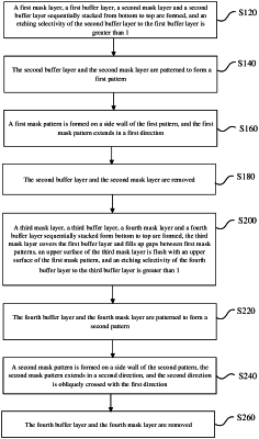
1. A method for manufacturing a semiconductor structure, comprising:
forming a first mask layer, a first buffer layer, a second mask layer and a second buffer layer sequentially stacked from bottom to top, wherein an etching selectivity of the second buffer layer to the first buffer layer is greater than 1;
patterning the second buffer layer and the second mask layer to form a first pattern;
forming a first mask pattern on a side wall of the first pattern, the first mask pattern extending in a first direction;
removing the second buffer layer and the second mask layer;
forming a third mask layer, a third buffer layer, a fourth mask layer and a fourth buffer layer sequentially stacked from bottom to top, wherein the third mask layer covers the first buffer layer and fills up gaps in the first mask pattern, an upper surface of the third mask layer is flush with an upper surface of the first mask pattern, and an etching selectivity of the fourth buffer layer to the third buffer layer is greater than 1;
patterning the fourth buffer layer and the fourth mask layer to form a second pattern;
forming a second mask pattern on a side wall of the second pattern, the second mask pattern extending in a second direction, and the second direction being obliquely crossed with the first direction; and
removing the fourth buffer layer and the fourth mask layer;
wherein before the first pattern is formed, the method further comprises: forming a fifth buffer layer on an upper surface of the second buffer layer, wherein a material of the fifth buffer layer is the same as that of the first buffer layer;
wherein patterning the second buffer layer and the second mask layer to form the first pattern comprises:
patterning the fifth buffer layer, wherein the first pattern is defined by a patterned fifth buffer layer;
patterning the second buffer layer based on the patterned fifth buffer layer to forming a patterned second buffer layer;
removing the patterned fifth buffer layer; and
patterning the second mask layer based on the patterned second buffer layer to form the first pattern.
|