| CPC H01L 21/0332 (2013.01) [H01L 21/31144 (2013.01)] | 14 Claims |
|
1. A method for fabricating a semiconductor structure, the semiconductor structure comprising a first region and a second region adjacent to each other, the method comprising:
forming a first pattern on the first region and forming a second pattern on the second region, the first pattern comprising a plurality of first sub-patterns, a first gap being provided between adjacent two of the plurality of first sub-patterns, a width of the first gap being a first pitch, the second pattern comprising a plurality of second sub-patterns, a second gap being provided between adjacent two of the plurality of second sub-patterns, a width of the second gap being a second pitch, the second pitch being greater than the first pitch;
forming a first mask layer on a sidewall of the first pattern, and forming a second mask layer on a sidewall of the second pattern, the first mask layer filling up the first gap, and the second mask layer not filling up the second gap;
removing the first pattern and the second pattern;
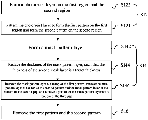
forming a mask pattern layer, the mask pattern layer covering a top and the sidewall of the first pattern and filling up the first gap, the mask pattern layer covering a top and the sidewall of the second pattern and a bottom of the second gap, a third gap being provided between each of the plurality of first sub-patterns and each of the plurality of second sub-patterns adjacent to each other, and the mask pattern layer also covering a bottom of the third gap; and
removing the mask pattern layer at the top of the first pattern, removing the mask pattern layer at the top of the second pattern and the mask pattern layer at the bottom of the second gap, and removing a portion of the mask pattern layer at the bottom of the third gap, to form the first mask layer in the first region and form the second mask layer in the second region; and,
wherein before removing the mask pattern layer at the top of the first pattern, removing the mask pattern layer at the top of the second pattern and the mask pattern layer at the bottom of the second gap, and removing a portion of the mask pattern layer at the bottom of the third gap, and the method further comprises:
reducing a thickness of the mask pattern layer, such that the thickness of the second mask layer is a target thickness, wherein the thickness of the mask pattern layer is reduced by means of a wet etching process.
|