| CPC H01L 21/0274 (2013.01) [G03F 7/70633 (2013.01); H01L 22/12 (2013.01)] | 20 Claims |
|
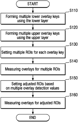
1. A method of manufacturing a semiconductor device, comprising:
forming a first lower overlay key including first and second patterns in a lower layer;
forming a first upper overlay key including third and fourth patterns in an upper layer vertically disposed on the lower layer;
irradiating a first measurement light to a first region of interest (ROI) over first portions of the first and second patterns to detect a first overlay error; and
irradiating a second measurement light to a second ROI over second portions of the first and second patterns, the second ROI being different from the first ROI, to detect a second overlay error, wherein the second measurement light has a different central frequency than the first measurement light.
|