US 12,068,156 B2
Selective deposition of SiOC thin films
Jan Willem Maes, Leuven (BE); David Kurt de Roest, Leuven (BE); and Oreste Madia, Leuven (BE)
Assigned to ASM IP Holding B.V., Almere (NL)
Filed by ASM IP HOLDING B.V., Almere (NL)
Filed on Apr. 24, 2023, as Appl. No. 18/305,875.
Application 18/305,875 is a continuation of application No. 17/463,813, filed on Sep. 1, 2021, granted, now 11,664,219.
Application 17/463,813 is a continuation of application No. 17/064,865, filed on Oct. 7, 2020, granted, now 11,139,163, issued on Oct. 5, 2021.
Claims priority of provisional application 62/928,978, filed on Oct. 31, 2019.
Prior Publication US 2023/0260782 A1, Aug. 17, 2023
This patent is subject to a terminal disclaimer.
Int. Cl. H01L 21/02 (2006.01); H01L 21/311 (2006.01)
CPC H01L 21/0228 (2013.01) [H01L 21/02126 (2013.01); H01L 21/02211 (2013.01); H01L 21/02274 (2013.01); H01L 21/31116 (2013.01)] 20 Claims
OG exemplary drawing
 
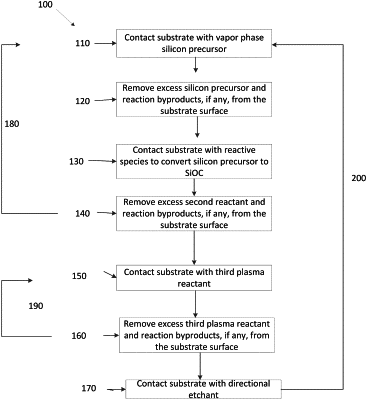
1. A method of selectively forming a silicon oxycarbide (SiOC) thin film on a dielectric surface of a substrate relative to a second surface of the substrate by a plasma enhanced atomic layer deposition (PEALD) process, wherein the PEALD process comprises at least one deposition cycle comprising:
contacting the substrate with a first vapor phase silicon reactant;
contacting the substrate with a second reactant comprising reactive species from a first plasma; and
contacting the substrate with a second plasma that is different from the first plasma.