| CPC H01L 21/02211 (2013.01) [H01L 29/0847 (2013.01); H01L 29/42392 (2013.01); H01L 29/66439 (2013.01); H01L 29/66742 (2013.01); H01L 29/04 (2013.01)] | 20 Claims |
|
1. A method of forming a semiconductor device comprising:
forming a multi-material layer on a substrate, wherein the multi-material layer includes a plurality of crystalline first layers and a plurality of non-crystalline second layers arranged in an alternating pattern;
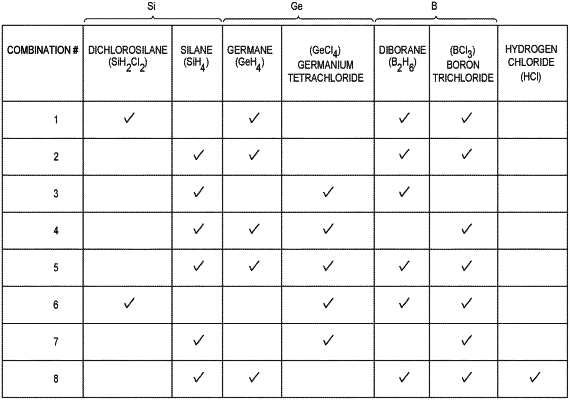
exposing the substrate and the multi-material layer to a gas mixture comprising:
a first precursor containing silicon;
a second precursor containing germanium; and
a third precursor containing a p-type dopant, wherein the second precursor, the third precursor, or both the second precursor and the third precursor further comprises chlorine; and
forming a source/drain layer on the substrate with predominantly <100> growth.
|