| CPC H01L 21/02087 (2013.01) [H01J 37/32385 (2013.01); H01J 37/3244 (2013.01); H01J 37/32532 (2013.01); H01L 21/02057 (2013.01)] | 9 Claims |
|
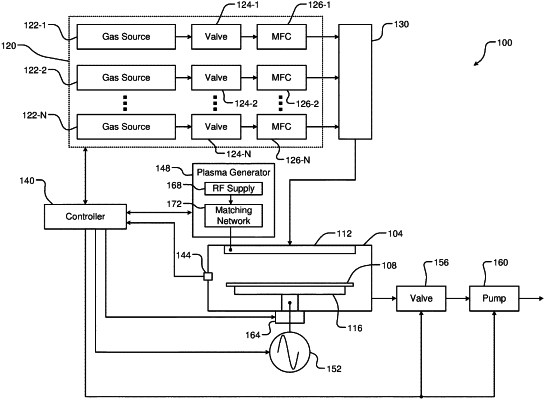
1. A system for performing a bevel cleaning process on a substrate, the system comprising:
a substrate support including an electrode, wherein at least a portion of the electrode is embedded within a dielectric; and
a plurality of plasma needles arranged around a perimeter of the substrate support, wherein the plasma needles are in fluid communication with a gas delivery system and are configured to (i) supply reactive gases from the gas delivery system to a bevel region of the substrate when the substrate is arranged on the substrate support and (ii) electrically couple to the electrode of the substrate support and generate plasma around the bevel region of the substrate.
|