| CPC H01G 4/30 (2013.01) [H01G 4/008 (2013.01); H01G 4/012 (2013.01); H01G 4/1218 (2013.01)] | 7 Claims |

|
1. A multilayer ceramic capacitor comprising:
a multilayer body including:
a laminate chip including an inner layer portion including dielectric layers and internal electrode layers laminated therein, and outer layer portions respectively provided on both side surfaces of the inner layer portion in a lamination direction;
side gap portions respectively provided on both side surfaces of the laminate chip in a width direction intersecting the lamination direction; and
external electrodes respectively provided on both side surfaces of the multilayer body in a length direction intersecting the lamination direction and the width direction, and each connected to the internal electrode layers; wherein
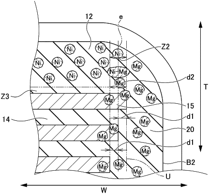
nickel and magnesium are segregated in a boundary region between the side gap portions and the outer layer portions.
|