| CPC H01G 4/015 (2013.01) [H01G 4/248 (2013.01); H01G 4/30 (2013.01)] | 15 Claims |
|
1. A multilayer electronic component comprising:
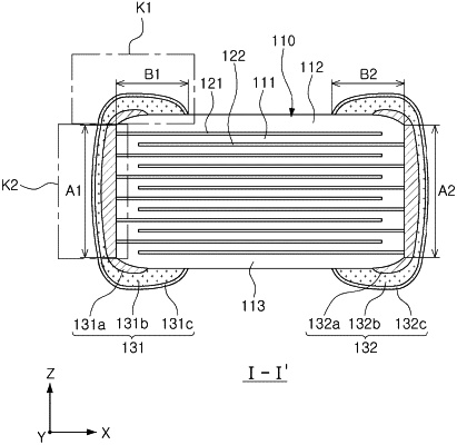
a body including first and second surfaces opposing each other in a first direction, third and fourth surfaces connected to the first and second surfaces and opposing each other in a second direction, and fifth and sixth surfaces connected to the first to fourth surfaces and opposing each other in a third direction and including a dielectric layer and internal electrodes alternately disposed with the dielectric layer interposed therebetween in the first direction; and
external electrodes disposed on the third and fourth surfaces,
wherein the external electrodes include an electrode layer disposed on the body and a conductive resin layer disposed on the electrode layer,
the conductive resin layer is in direct contact with the electrode layer and includes a conductive metal and an epoxy resin, and
the external electrodes include connection portions disposed on the third surface and the fourth surface and band portions extending from the connection portions to the first and second surfaces, and an average thickness of the conductive resin layer at the connection portion is smaller than an average thickness of the conductive resin layer at the band portion.
|