| CPC H01G 11/48 (2013.01) [H01G 11/52 (2013.01); H01G 11/54 (2013.01); H01M 4/608 (2013.01); H01M 2004/028 (2013.01)] | 3 Claims |
|
1. An electrochemical device electrode comprising a conductive polymer as an active material, wherein:
the conductive polymer has a grain shape and contains polyanilines,
an intensity distribution pattern obtained by X-ray diffraction measurement with respect to the conductive polymer has a first peak in which a diffraction angle 2θ ranges from 18° to 21°, inclusive, and a second peak in which a diffraction angle 2θ ranges from 24° to 26º, inclusive, and
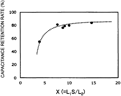
the conductive polymer satisfies a relational expression: 7.6≤L1·S/L2≤14.6,
where L1 represents a crystallite size (nm) corresponding to the first peak, L2 represents a crystallite size (nm) corresponding to the second peak, and S represents the specific surface area (m2/g) of the conductive polymer.
|