| CPC H01F 27/2804 (2013.01) [H01F 27/2885 (2013.01); H01L 23/49838 (2013.01); H01L 23/552 (2013.01); H01L 23/58 (2013.01); H01F 2027/2809 (2013.01); H01F 37/00 (2013.01); H01L 23/49822 (2013.01)] | 14 Claims |

|
1. An electronic package comprising:
an integrated circuit (IC) configured to receive a power input signal and to deliver a regulated power output signal;
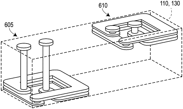
a multilayer electrical routing structure attached to the IC and configured to couple the electronic package to an external circuit, the multilayer electrical routing structure having one or more electrical conductors on each of at least two layers configured to route the power input signal from the external circuit to the IC and to route the regulated power output signal from the IC to the external circuit, wherein the one or more electrical conductors form an integrated inductive device having a first portion of a turn formed on a first layer of the at least two layers and a second portion of the turn formed on a second layer of the at least two layers, wherein the first portion is connected in series to the second portion through one or more vias, wherein a central axis of the integrated inductive device is oriented perpendicular to the at least two layers and wherein the power output signal is coupled to the external circuit through the integrated inductive device; and
an encapsulant formed over the IC and at least a portion of the multilayer electrical routing structure.
|