| CPC G11C 7/1093 (2013.01) [G11C 7/1048 (2013.01); G11C 7/1066 (2013.01); G11C 7/12 (2013.01); G11C 8/08 (2013.01); G11C 8/18 (2013.01)] | 20 Claims |
|
1. A static random access memory (SRAM) controller, comprising:
a host interface configured to:
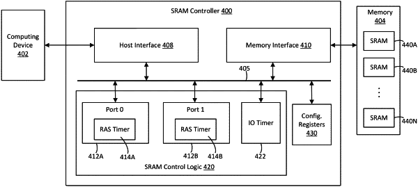
provide a port through which one or more memory requests are received from a computing device external to the SRAM controller, each memory request specifying a corresponding memory address for a read or write access to an SRAM device external to the SRAM controller, and
generate a set of burst accesses based on the one or more memory requests, the set of burst accesses comprising encoded addresses for input to a plurality of internal ports of the SRAM controller in parallel;
first control logic configured to generate a first plurality of control signals for output to [an] the SRAM device through a memory interface communicatively coupling the SRAM device to the SRAM controller, wherein the first plurality of control signals causes a first group of bit cells in the SRAM device to be accessed in sequential address order, and wherein the first plurality of control signals includes a first decoded row address, a first precharge signal, and a first column select signal;
a first row address strobe (RAS) timer configured to generate a clock signal controlling a timing of the first precharge signal, wherein the first precharge signal triggers a precharge operation during a first RAS phase in which the first control logic performs a word line decoding operation once for all bit cells in the first group of bit cells to output the first decoded row address; and
an input/output (IO) timer configured to generate a clock signal controlling a timing of the first column select signal, wherein the first column select signal is updated multiple times during a first IO phase that follows the first RAS phase, each update to the first column select signal causing a different bit cell in the first group of bit cells to be selected.
|