| CPC G11C 16/3459 (2013.01) [G11C 16/0433 (2013.01); G11C 16/08 (2013.01); G11C 16/102 (2013.01); G11C 16/14 (2013.01); G11C 16/26 (2013.01); G11C 16/30 (2013.01); G11C 16/3445 (2013.01)] | 24 Claims |

|
1. A semiconductor memory device comprising:
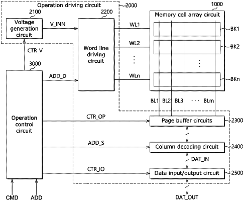
a memory cell array circuit including a plurality of memory cells that are coupled to a plurality of word lines; and
a driving force adjustment circuit configured to adjust, based on a location of a verify target memory cell, driving forces of a plurality of respective verify pass voltages that are applied to unselected word lines among the plurality of word lines,
wherein each of the verify pass voltages reaches a corresponding target voltage level more quickly as a corresponding driving force increases.
|