| CPC G11C 16/30 (2013.01) [G11C 16/0483 (2013.01)] | 12 Claims |

|
1. A semiconductor memory device comprising:
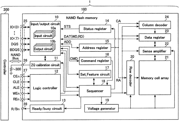
a memory cell array including a memory cell configured to store data;
a sense amplifier connected to the memory cell;
a data register connected to the sense amplifier;
an input/output circuit connected to the data register; and
a pad group connected to the input/output circuit,
wherein
the pad group includes
a first power supply pad to which a first voltage is supplied;
a second power supply pad to which a second voltage different from the first voltage is supplied; and
a first input/output pad, and
the input/output circuit includes
a first circuit unit supplied with the first voltage and the second voltage, and configured to receive a first signal from the data register and output a second signal predicated on the first signal;
a second circuit unit supplied with the first voltage and the second voltage, and configured to receive the second signal and output a third signal predicated on the second signal;
a first driver circuit configured to receive a fourth signal predicated on the third signal and output a fifth signal predicated on the fourth signal toward the first input/output pad;
a first interconnect connected between the first circuit unit and the first power supply pad; and
a second interconnect connected between the second circuit unit and the first power supply pad, the second interconnect being physically separated from the first interconnect.
|