US 12,068,040 B2
Nonvolatile semiconductor memory device including a memory cell array and a control circuit applying a reading voltage
Yasuhiro Shiino, Yokohama Kanagawa (JP); Eietsu Takahashi, Yokohama Kanagawa (JP); and Koki Ueno, Yokohama Kanagawa (JP)
Assigned to KIOXIA CORPORATION, Tokyo (JP)
Filed by KIOXIA CORPORATION, Tokyo (JP)
Filed on Sep. 15, 2023, as Appl. No. 18/467,793.
Application 18/467,793 is a continuation of application No. 18/173,211, filed on Feb. 23, 2023, granted, now 11,817,155.
Application 18/173,211 is a continuation of application No. 17/219,003, filed on Mar. 31, 2021, granted, now 11,621,041, issued on Apr. 4, 2023.
Application 17/219,003 is a continuation of application No. 17/026,904, filed on Sep. 21, 2020, granted, now 11,004,520, issued on May 11, 2021.
Application 17/026,904 is a continuation of application No. 16/597,242, filed on Oct. 9, 2019, granted, now 10,818,362, issued on Oct. 27, 2020.
Application 16/597,242 is a continuation of application No. 16/209,520, filed on Dec. 4, 2018, granted, now 10,490,286, issued on Nov. 26, 2019.
Application 16/209,520 is a continuation of application No. 15/915,129, filed on Mar. 8, 2018, granted, now 10,186,321, issued on Jan. 22, 2019.
Application 15/915,129 is a continuation of application No. 15/598,554, filed on May 18, 2017, granted, now 9,947,415, issued on Apr. 17, 2018.
Application 15/598,554 is a continuation of application No. 15/263,518, filed on Sep. 13, 2016, granted, now 9,691,489, issued on Jun. 27, 2017.
Application 15/263,518 is a continuation of application No. 14/677,111, filed on Apr. 2, 2015, granted, now 9,472,295, issued on Oct. 18, 2016.
Application 14/677,111 is a continuation of application No. 14/088,744, filed on Nov. 25, 2013, granted, now 9,025,387, issued on May 5, 2015.
Application 14/088,744 is a continuation of application No. 13/749,029, filed on Jan. 24, 2013, granted, now 8,649,221, issued on Feb. 11, 2014.
Application 13/749,029 is a continuation of application No. 13/246,004, filed on Sep. 27, 2011, granted, now 8,385,126, issued on Feb. 26, 2013.
Claims priority of application No. 2011-084762 (JP), filed on Apr. 6, 2011.
Prior Publication US 2024/0005999 A1, Jan. 4, 2024
This patent is subject to a terminal disclaimer.
Int. Cl. G11C 16/10 (2006.01); G11C 11/56 (2006.01); G11C 16/04 (2006.01); G11C 16/08 (2006.01); G11C 16/14 (2006.01); G11C 16/26 (2006.01); G11C 16/34 (2006.01)
CPC G11C 16/26 (2013.01) [G11C 11/5628 (2013.01); G11C 16/0483 (2013.01); G11C 16/08 (2013.01); G11C 16/10 (2013.01); G11C 16/14 (2013.01); G11C 16/3427 (2013.01); G11C 16/349 (2013.01)] 20 Claims
OG exemplary drawing
 
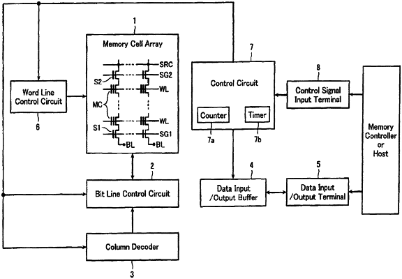
1. A nonvolatile semiconductor memory device comprising:
a memory cell array which comprises: a memory string having a plurality of memory cells connected in series therein; a first select transistor connected to one end of the memory string; a second select transistor connected to the other end of the memory string; a bit line connected to the memory string via the first select transistor; a source line connected to the memory string via the second select transistor; and a word line connected to a control gate electrode of each of the memory cells; and
a control circuit configured to apply a reading voltage to the control gate electrode of a selected memory cell in the memory string to determine whether the selected memory cell is conductive or not while applying to the control gate electrode of a non-selected memory cell in the memory string a reading pass voltage for rendering the non-selected memory cell conductive regardless of data stored in the non-selected memory cell, and thereby performing a reading operation for the selected memory cell,
the control circuit being configured to
in a first stage of the reading operation, apply a first reading voltage to a selected word line connected to the control gate electrode of the selected memory cell and apply a first reading pass voltage to a first non-selected word line connected to the control gate electrode of a first non-selected memory cell, and
in a second stage subsequent to the first stage of the reading operation, apply a second reading voltage to the selected word line and apply to the first non-selected word line a second reading pass voltage of which voltage value is different from that of the first reading pass voltage.