| CPC G11C 16/26 (2013.01) [G11C 11/5642 (2013.01); G11C 11/5671 (2013.01)] | 20 Claims |

|
1. A memory device, comprising:
a memory block including a plurality of memory cells that are coupled to a plurality of word lines;
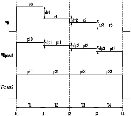
a peripheral circuit configured to perform a read operation by applying a read voltage to a selected word line, among the plurality of word lines, and applying a first pass voltage to target word lines, wherein the target word lines are adjacent to the selected word line, among unselected word lines other than the selected word line; and
a control logic configured to:
decrease the read voltage based on a read voltage variation; and
decrease the first pass voltage based on a pass voltage variation when the read voltage decreases,
wherein the pass voltage variation is less than the read voltage variation.
|