| CPC G11C 16/16 (2013.01) [G11C 16/26 (2013.01); G11C 16/32 (2013.01)] | 20 Claims |
|
1. A memory device comprising:
a memory array comprising memory cells; and
control logic operatively coupled with the memory array, the control logic to perform operations comprising:
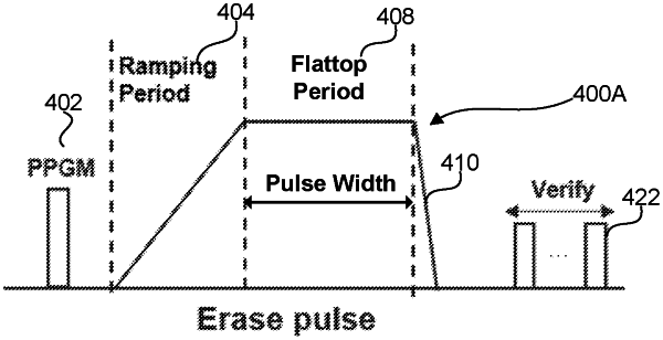
causing a first erase pulse to be applied to a memory line of the memory array to perform an erase operation, the memory line being a conductive line coupled to a string of the memory cells;
suspending the erase operation in response to receipt of a suspend command during a ramping period of the first erase pulse;
recording a suspend voltage level of the first erase pulse when suspended;
causing the erase operation to be resumed in response to an erase resume command;
selectively modifying a pulse width of a flattop period of a second erase pulse based on the suspend voltage level; and
causing the second erase pulse to be applied to the memory line during a resume of the erase operation.
|