| CPC G11C 16/102 (2013.01) [G11C 16/0433 (2013.01); G11C 16/3404 (2013.01); G11C 16/3459 (2013.01)] | 20 Claims |

|
1. A memory device, comprising:
a plurality of memory cells coupled to a plurality of bit lines and a common source line, the plurality of memory cells forming a plurality of strings respectively coupled to the plurality of bit lines and coupled in common to the common source line, each string including a drain select transistor, a portion of the plurality of memory cells, and a source select transistor that are coupled in series to each other; and
a control circuit configured to control a peripheral circuit to perform a program operation that includes two or more program steps on selected memory cells of a selected word line, among word lines,
wherein the peripheral circuit is configured to:
perform a first program step of the two or more program steps on the selected memory cells;
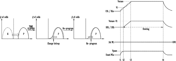
perform a detrap operation that applies a detrap voltage to the plurality of bit lines and the common source line for a predefined time, and controls a drain select line coupled to the drain select transistor and a source select line coupled to the source select transistor to float; and
perform a second program step of the two or more program steps on the selected memory cells.
|