US 12,068,032 B2
Device-region layout for embedded flash
Shih Kuang Yang, Tainan (TW); Ping-Cheng Li, Kaohsiung (TW); Hung-Ling Shih, Tainan (TW); Po-Wei Liu, Tainan (TW); Wen-Tuo Huang, Tainan (TW); Yu-Ling Hsu, Tainan (TW); Yong-Shiuan Tsair, Tainan (TW); and Chia-Sheng Lin, Tainan (TW)
Assigned to Taiwan Semiconductor Manufacturing Company, Ltd., Hsinchu (TW)
Filed by Taiwan Semiconductor Manufacturing Company, Ltd., Hsin-Chu (TW)
Filed on May 23, 2023, as Appl. No. 18/321,975.
Application 16/952,411 is a division of application No. 16/400,361, filed on May 1, 2019, granted, now 10,861,553, issued on Dec. 8, 2020.
Application 18/321,975 is a continuation of application No. 17/506,904, filed on Oct. 21, 2021, granted, now 11,699,488.
Application 17/506,904 is a continuation of application No. 16/952,411, filed on Nov. 19, 2020, granted, now 11,158,377, issued on Oct. 26, 2021.
Claims priority of provisional application 62/737,288, filed on Sep. 27, 2018.
Prior Publication US 2023/0290411 A1, Sep. 14, 2023
This patent is subject to a terminal disclaimer.
Int. Cl. G11C 16/08 (2006.01); G11C 11/16 (2006.01); H10B 12/00 (2023.01); H10B 41/30 (2023.01)
CPC G11C 16/08 (2013.01) [G11C 11/1657 (2013.01); H10B 12/053 (2023.02); H10B 41/30 (2023.02)] 20 Claims
OG exemplary drawing
 
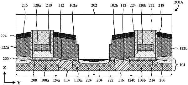
1. An integrated chip comprising:
a substrate;
a first source/drain region in the substrate;
an erase gate, a control gate, and a word line overlying the substrate, wherein the control gate is between and borders the erase gate and the word line, and wherein the word line is between and borders the control gate and the first source/drain region;
a silicide layer atop the first source/drain region; and
a trench isolation structure underlying the word line;
wherein a bottom surface of the word line is recessed into a top surface of the trench isolation structure to an elevation, which is recessed relative to a top surface of the silicide layer.