| CPC G11C 13/0069 (2013.01) [G11C 13/0026 (2013.01); G11C 13/0028 (2013.01); G11C 13/0038 (2013.01); G11C 13/004 (2013.01); G11C 13/0064 (2013.01); G11C 13/0097 (2013.01); G11C 13/0002 (2013.01); G11C 13/003 (2013.01); G11C 2013/0078 (2013.01); G11C 2213/79 (2013.01); G11C 2213/82 (2013.01)] | 9 Claims |

|
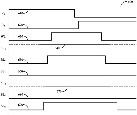
1. A resistive random-access memory (ReRAM) array with parallel reset and set programming comprising:
a plurality of ReRAM cells arranged in an array, wherein the array includes a plurality of rows and a plurality of columns, wherein at least two ReRAM cells of the array includes a word, wherein each ReRAM cell includes a select device having a control port, a first port, and a second port, such that under a control of a signal applied to the control port, current is configured to flow or not flow between the first port and the second port, and a resistive element including a top electrode (TE) and a bottom electrode (BE), wherein the control port is connected to a word line, the first port connected to a source line, the TE connected to a bit line, and the second port is connected to the BE; and
a plurality of controllers, wherein an output of each of the plurality of controllers causes a reset programming or a set programming of a ReRAM cell in a column of the plurality of ReRAM cells that has a respective word line activated;
such that the reset programming and the set programming occur in parallel,
wherein each of the plurality of the controllers further comprises:
a first set/reset (SR) signal input, wherein the first SR signal input is configured to receive a first SR signal that is at any one of: a first operational level and a second operational level;
a first output communicatively connected to the source line of the column of the plurality of ReRAM cells;
a second output communicatively connected to the bit line of the column of the plurality of ReRAM cells;
a first multiplexer having a first input connected to a first voltage source and a second input connected to the first SR signal input, wherein upon the first SR signal presenting the first operational level, the first voltage source is connected to the first output and upon the first SR signal presenting the second operational level, the first voltage source is connected to the second output; and
a second multiplexer having a third input connected to a second voltage source and a fourth input connected to the first SR signal input, wherein upon the first SR signal presenting the first operational level, the second voltage source is connected to the second output and upon the first SR signal presenting the second operational level, the second voltage source is connected to the first output.
|