| CPC G11C 11/4074 (2013.01) [G11C 11/406 (2013.01); G11C 11/4085 (2013.01); G11C 11/4091 (2013.01); G11C 11/4094 (2013.01)] | 23 Claims |

|
1. A DRAM chip, comprising:
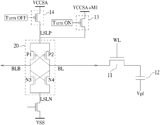
a first sustaining voltage generator producing a first voltage level which is higher than a voltage level of the signal ONE utilized in the DRAM chip;
a first supplying voltage source generating the voltage level corresponding to signal ONE utilized in the DRAM chip, wherein the first sustaining voltage generator and the first supplying voltage source are physically separate each other;
a DRAM cell comprising an access transistor and a storage capacitor;
a sense amplifier coupled to a bit line and a complementary bit line, wherein the bit line is coupled to the storage capacitor through the access transistor; wherein the sense amplifier is selectively coupled to the first sustaining voltage generator and the first supplying voltage source and does not simultaneously receive the voltage level and the first voltage level;
an equalization circuit coupled to the bit line and the complementary bit line, wherein the equalization circuit couples the bit line and the complementary bit line to a preset reference voltage during an equalization period; and
a clean up circuit coupled to the sense amplifier or the equalization circuit;
wherein the first sustaining voltage generator is electrically coupled to the bit line during a turning-off period of the access transistor, and the clean up circuit generates a clean up pulse to mitigate a difference between a voltage of the bit line and a preset reference voltage during the equalization period, a width of the clean up pulse depends on a restore voltage, and the restore voltage is higher than a voltage level of a signal ONE utilized in the DRAM chip.
|