| CPC G11C 11/4072 (2013.01) [G11C 11/4074 (2013.01); G11C 11/4076 (2013.01); G11C 11/4099 (2013.01)] | 8 Claims |

|
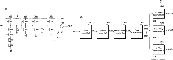
1. A semiconductor integrated circuit, comprising:
a plurality of planes, each of the planes including at least one memory bank; and
an internal voltage generation block individually providing an internal voltage to each of the plurality of planes,
wherein the internal voltage generation block includes:
an enable control circuit configured to generate a final enable signal by delaying a re-enable timing of an enable signal;
a start-up control circuit configured to generate a start-up signal to perform a reset operation during a reset time using a delayed final enable signal;
a reference voltage generation circuit configured to generate a reference voltage using the start-up signal; and
a voltage generation circuit configured to generate a plurality of internal voltages applied to each of the plurality of planes based on the reference voltage,
wherein the start-up control circuit includes:
a delay circuit configured to generate the delayed final enable signal by delaying the final enable signal by a preset delay time; and
an output circuit configured to output the start-up signal having a pulse width corresponding to the preset delay time, based on the delayed final enable signal.
|