| CPC G11C 11/4072 (2013.01) [G11C 5/06 (2013.01); G11C 5/14 (2013.01); G11C 11/4074 (2013.01)] | 20 Claims |

|
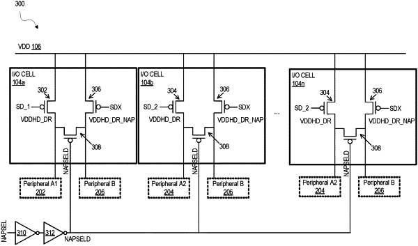
1. A memory I/O system, comprising:
a first header circuit configured to receive a power supply voltage signal and having a first output terminal configured to provide a first output voltage signal in a first power domain to a first plurality of peripheral circuits;
a second header circuit configured to receive the power supply voltage signal and having a second output terminal configured to provide a second output voltage signal in a second power domain to a second plurality of peripheral circuits;
a control switch connected between the first and second header circuits, wherein when switching from a sleep mode to a wake-up mode, the control switch is configured to selectively provide the first output voltage signal in the first power domain to at least a portion of the second plurality of peripheral circuits without turning on the second header circuit.
|