| CPC G11C 11/1675 (2013.01) [G11C 8/10 (2013.01); G11C 11/1655 (2013.01); G11C 11/1657 (2013.01)] | 20 Claims |
|
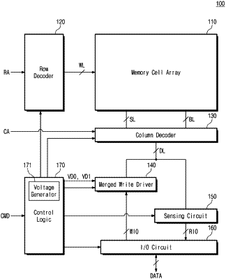
1. A memory device, comprising:
a memory cell array including a first sub memory cell array including a first memory cell and a second sub memory cell array including a second memory cell;
a merged write driver including a first write circuit configured to receive n-bit data (n being a natural number of 2 or more) through a write input/output line, to output a first write voltage to a merged node in response to a first data bit of the n-bit data, and to output a second write voltage to the merged node in response to a second data bit of the n-bit data; and
a column decoder including a first column multiplexer configured to apply a first voltage of the merged node corresponding to the first data bit to the first memory cell, and including a second column multiplexer configured to apply a second voltage of the merged node corresponding to the second data bit to the second memory cell.
|