| CPC G11C 11/161 (2013.01) [G11B 5/3912 (2013.01); G11C 11/1659 (2013.01); H10B 61/22 (2023.02); H10N 50/01 (2023.02); H10N 50/10 (2023.02)] | 20 Claims |
|
1. A semiconductor apparatus comprising a nonvolatile memory cell array including:
a plurality of first memory cells, each of the plurality of first memory cells including a first memory element including a resistance-variable nonvolatile memory element and a first selection transistor electrically connected to the first memory element, and
a plurality of second memory cells, each of the plurality of second memory cells including a second memory element including a resistance-variable nonvolatile memory element and a second selection transistor electrically connected to the second memory element, wherein
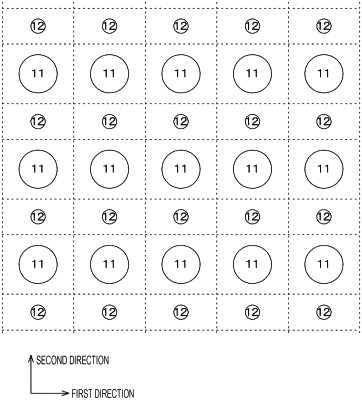
a plurality of first memory elements and a plurality of second memory elements are arranged in a two-dimensional matrix in a first direction and a second direction different from the first direction and on a same interlayer insulating layer,
the first memory element is larger than the second memory element, and
the first memory element and the second memory element are disposed adjacent to each other along the second direction.
|