| CPC G11B 5/3146 (2013.01) [G11B 5/11 (2013.01); G11B 5/1278 (2013.01); G11B 5/235 (2013.01); G11B 5/3133 (2013.01); G11B 5/314 (2013.01); G11B 5/3163 (2013.01); G11B 2005/0024 (2013.01); G11B 5/3912 (2013.01); G11B 5/3919 (2013.01); G11B 2005/3996 (2013.01)] | 14 Claims |

|
1. A method of manufacturing a transfer torque reversal assisted magnetic recording (STRAMR) structure, the method comprising:
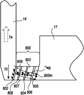
providing a main pole (MP) that is configured to generate a write field which is directed through a pole tip at an air bearing surface (ABS), and to generate a write gap (WG) field in a down-track direction across a spin torque oscillator (STO) device in a WG, and between a MP trailing side and a trailing shield (TS);
disposing the trailing shield (TS) with a side at the ABS, and a bottom surface facing the MP; and
providing the STO device, comprising:
(1) a flux guiding layer that has a negative spin polarization (nFGL), wherein the nFGL comprises a magnetization pointing substantially parallel to the WG field without a current bias and formed between a first spin polarization preserving layer (ppL1) and a second spin polarization preserving layer (ppL2);
(2) a positive spin polarization (pSP) layer that adjoins the TS bottom surface;
(3) a non-spin polarization preserving layer (pxL) contacting the MP trailing side;
(4) a first negative spin injection layer (nSIL1) between the ppL2 and a third spin polarization preserving layer (ppL3); and
(5) a second negative spin injection layer (nSIL2) between the ppL3 and the pxL, wherein the nFGL, nSIL1, and nSIL2 have a spin polarization that is negative; and
applying a direct current (DC) of sufficient current density (J) from the TS to MP across the STO device, wherein the magnetization of the nFGL is configured to flip to a direction substantially antiparallel to the WG field, wherein the nSIL1 and nSIL2 are configured to exert an additive spin torque on the nFGL to cause a magnetization of the nFGL to flip to a direction substantially antiparallel to the WG field thereby increasing reluctance in the WG and enhancing the write field, and wherein the nSIL1 and nSIL2 have a saturation magnetization×thickness (Mst) product substantially less than that of the nFGL.
|