| CPC G09G 3/3696 (2013.01) [G09G 3/3258 (2013.01); G09G 3/3648 (2013.01); G09G 2310/0286 (2013.01); G09G 2310/0291 (2013.01); G09G 2320/0252 (2013.01); G09G 2320/0276 (2013.01); G09G 2320/0626 (2013.01)] | 6 Claims |
|
1. A display driver that generates a drive signal for driving a display device in response to a pixel data piece that represents a luminance level of each pixel based on a video signal, the display driver comprising:
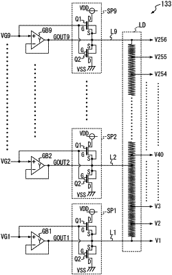
a gradation voltage generation unit that includes first to k-th (k is an integer of 2 or more) amplifiers to which first to k-th reference voltages having mutually different voltage values are individually input, the first to k-th amplifiers amplifying the first to k-th reference voltages and outputting the amplified first to k-th reference voltages, the gradation voltage generation unit generating a plurality of gradation voltages by dividing the voltages between respective voltages output from the first to k-th amplifiers; and
a decoder unit that selects one gradation voltage corresponding to the luminance level represented by the pixel data piece among the plurality of gradation voltages and generates a signal having the one gradation voltage as the drive signal, wherein
the gradation voltage generation unit includes a plurality of response-speed increase circuits connected to respective first to k-th amplifiers, and
each of the response-speed increase circuits includes at least one transistor wherein a source and a back gate of the at least one transistor are directly connected to an output terminal of the amplifier, a predetermined electric potential is applied to a drain of the at least one transistor, and the reference voltage input to the amplifier is applied to a gate of the at least one transistor.
|