| CPC G09G 3/3233 (2013.01) [G09G 2300/0842 (2013.01); G09G 2310/061 (2013.01); G09G 2320/0233 (2013.01); G09G 2320/0247 (2013.01)] | 20 Claims |
|
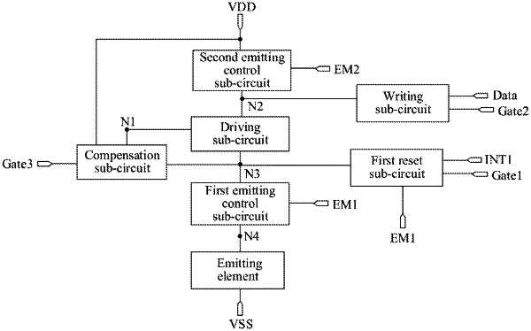
1. A pixel circuit, comprising a driving sub-circuit, a writing sub-circuit, a compensation sub-circuit, a first reset sub-circuit, and an emitting element,
wherein
the driving sub-circuit is connected with a first node, a second node, and a third node respectively, and is configured to provide a driving current for the third node under control of signals of the first node and the second node;
the writing sub-circuit is connected with a second scanning signal terminal, a data signal terminal, and the second node respectively, and is configured to write a signal of the data signal terminal into the second node under control of a signal of the second scanning signal terminal;
the first reset sub-circuit is connected with a first scanning signal terminal, a first emitting control signal terminal, a first initial signal terminal, and the third node respectively, and is configured to write an initial voltage signal of the first initial signal terminal into the third node under control of signals of the first scanning signal terminal and the first emitting control signal terminal;
the compensation sub-circuit is connected with a first voltage terminal, a third scanning signal terminal, the first node, and the third node respectively, and is configured to write the initial voltage signal of the third node into the first node under control of a signal of the third scanning signal terminal and compensate the first node under control of the signal of the third scanning signal terminal; and
one terminal of the emitting element is connected with a fourth node, while the other terminal is connected with a second voltage terminal.
|