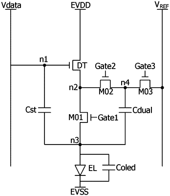
| CPC G09G 3/3233 (2013.01) [G09G 3/3291 (2013.01); G09G 2300/0852 (2013.01); G09G 2320/0233 (2013.01)] | 22 Claims |

|
1. A pixel circuit, comprising:
a driving element including a gate connected directly to a first node to which a data voltage is configured to be applied, a first electrode connected to a high-potential voltage line, and a second electrode connected to a second node;
a first switch element connected between the second node and a third node;
a second switch element connected between the second node and a fourth node;
a third switch element connected between the fourth node and a reference voltage line;
a first capacitor connected between the first node and the third node, the first capacitor including an electrode connected directly to the first node and another electrode connected directly to the third node; and
a second capacitor connected between the third node and the fourth node, the second capacitor including an electrode connected directly to the third node and another electrode connected directly to the fourth node,
wherein the second switch element includes a gate configured to receive a first signal, and the third switch element includes a gate configured to receive a second signal different from the first signal.
|