| CPC G09G 3/3233 (2013.01) [G09G 2300/0452 (2013.01); G09G 2300/0819 (2013.01); G09G 2300/0842 (2013.01); G09G 2310/0202 (2013.01); G09G 2310/0297 (2013.01); G09G 2310/08 (2013.01)] | 2 Claims |
|
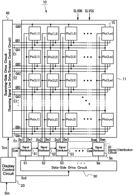
1. A method for driving a display device including a plurality of data signal lines, a plurality of scanning signal lines intersecting the plurality of data signal lines, and a plurality of pixel circuits arranged along the plurality of data signal lines and the plurality of scanning signal lines, the method comprising:
a data-side driving step of outputting a plurality of data signals representing an image to be displayed;
a signal distribution step of receiving the plurality of data signals and providing the plurality of data signals to the plurality of data signal lines; and
a scanning-side driving step of selectively driving the plurality of scanning signal lines such that a selection period of each of the scanning signal lines has a portion overlapping with a selection period of a scanning signal line to be selected next; wherein
the plurality of pixel circuits define a plurality of pixel circuit columns extending along the plurality of data signal lines,
the plurality of scanning signal lines are respectively connected to ones of the plurality of pixel circuits defining each of the plurality of pixel circuit columns, the plurality of pixel circuit columns are arranged such that two-color pixel circuit columns each having a first color pixel circuit and a second color pixel circuit arranged alternately and monochromatic pixel circuit columns each having only third color pixel circuits are alternately arranged in a direction in which the plurality of scanning signal lines extend,
the plurality of data signal lines include a plurality of two-color data signal line groups that are a plurality of data signal line groups with two data signal lines as one group and respectively correspond to a plurality of two-color pixel circuit columns in the plurality of pixel circuit columns, and a plurality of monochromatic data signal lines that respectively correspond to a plurality of monochromatic pixel circuit columns in the plurality of pixel circuit columns,
a first color pixel circuit and a second color pixel circuit included in each two-color pixel circuit column in the plurality of pixel circuit columns are respectively connected to one and the other of two data signal lines in a data signal line group corresponding to the each two-color pixel circuit column, and all pixel circuits included in each monochrome pixel circuit column in the plurality of pixel circuit columns are connected to one data signal line corresponding to the each monochrome pixel circuit column,
the plurality of data signals correspond to the plurality of pixel circuit columns, respectively,
in the signal distribution step, a data signal corresponding to each two-color pixel circuit column in the plurality of pixel circuit columns is distributed to two data signal lines in a data signal line group corresponding to the each two-color pixel circuit column,
a data signal corresponding to each monochrome pixel circuit column in the plurality of pixel circuit columns is provided to one data signal line corresponding to the each monochrome pixel circuit column, and
one data signal among the plurality of data signals is distributed to the two data signal lines such that for each pixel circuit connected to each data signal line of the two data signal lines, the one data signal is applied to the each data signal line in a first period that is included in a corresponding selection period and does not overlap with a following selection period, and such that a voltage of the one data signal applied in the first period is held in the each data signal line with capacitance thereof by electrically disconnecting the each data signal line from the one data signal in a second period that is included in the corresponding selection period and overlaps with the following selection period, wherein the corresponding selection period is a selection period of a scanning signal line connected to the each pixel circuit, and the following selection period is a selection period of a scanning signal line to be selected next.
|