US 12,067,934 B2
Display device and electronic device including display device
Shunpei Yamazaki, Setagaya (JP); Jun Koyama, Sagamihara (JP); and Hiroyuki Miyake, Atsugi (JP)
Assigned to Semiconductor Energy Laboratory Co., Ltd., Atsugi (JP)
Filed by Semiconductor Energy Laboratory Co., Ltd., Atsugi (JP)
Filed on Aug. 25, 2021, as Appl. No. 17/411,401.
Application 17/411,401 is a continuation of application No. 16/862,658, filed on Apr. 30, 2020, granted, now 11,107,396.
Application 16/862,658 is a continuation of application No. 16/130,447, filed on Sep. 13, 2018, granted, now 10,657,882, issued on May 19, 2020.
Application 16/130,447 is a continuation of application No. 14/881,500, filed on Oct. 13, 2015, granted, now 10,083,651, issued on Sep. 25, 2018.
Application 14/881,500 is a continuation of application No. 14/540,326, filed on Nov. 13, 2014, granted, now 9,165,502, issued on Oct. 20, 2015.
Application 14/540,326 is a continuation of application No. 12/906,538, filed on Oct. 18, 2010, granted, now 8,890,781, issued on Nov. 18, 2014.
Claims priority of application No. 2009-242757 (JP), filed on Oct. 21, 2009; and application No. 2009-278997 (JP), filed on Dec. 8, 2009.
Prior Publication US 2021/0383750 A1, Dec. 9, 2021
Int. Cl. G09G 3/3208 (2016.01); G09G 3/20 (2006.01); G09G 3/3233 (2016.01); H01L 27/12 (2006.01); H01L 29/786 (2006.01); H10K 59/121 (2023.01); H10K 59/131 (2023.01)
CPC G09G 3/3208 (2013.01) [G09G 3/2003 (2013.01); G09G 3/3233 (2013.01); H01L 27/1225 (2013.01); H01L 29/78609 (2013.01); H01L 29/7869 (2013.01); H01L 29/78693 (2013.01); H01L 29/78696 (2013.01); H10K 59/1213 (2023.02); H10K 59/131 (2023.02); G09G 2330/021 (2013.01)] 18 Claims
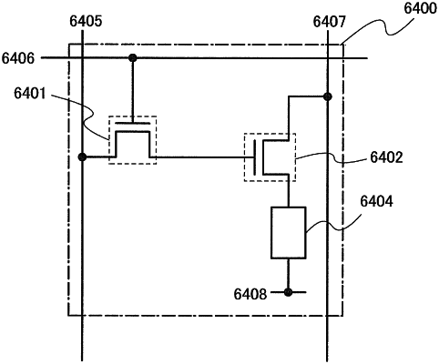
OG exemplary drawing
 
1. A display device configured to reduce a frequency of writing of image signals to a pixel portion in a period in which a still image is displayed in the pixel portion,
wherein the pixel portion comprises a light-emitting element and a switching transistor in a pixel,
wherein the switching transistor is configured to control an input of the image signals to the pixel,
wherein the switching transistor comprises an oxide semiconductor layer, and
wherein an off-state current of the switching transistor is 1×10⁻¹³ A or less.