| CPC G09G 3/006 (2013.01) [G09G 3/32 (2013.01); G09G 2300/0413 (2013.01); G09G 2300/0426 (2013.01); G09G 2300/0819 (2013.01); G09G 2300/0842 (2013.01); G09G 2300/0861 (2013.01); G09G 2320/0233 (2013.01); G09G 2320/0242 (2013.01); G09G 2330/08 (2013.01); G09G 2330/12 (2013.01)] | 20 Claims |
|
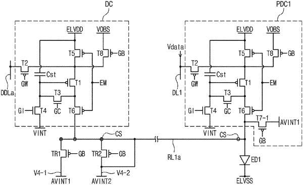
1. A display device comprising:
a plurality of pixels in a display area;
a dummy pixel in a dummy area adjacent to the display area; and
a repair line connectable with the dummy pixel and each of the plurality of pixels,
wherein the plurality of pixels comprise:
a first subpixel comprising a first pixel circuit connected with a first initialization voltage line configured to provide a first initialization voltage, and a first light emitting element adjacent to the first pixel circuit and configured to emit first light; and
a second subpixel comprising a second pixel circuit connected with a second initialization voltage line configured to provide a second initialization voltage different from the first initialization voltage, and a second light emitting element adjacent to the second pixel circuit and configured to emit second light different from the first light, and
wherein the dummy pixel comprises:
a first transistor connectable with the repair line and connected with the first initialization voltage line;
a second transistor connectable with the repair line and connected with the second initialization voltage line; and
a dummy pixel circuit connectable with the repair line.
|