| CPC G06V 40/1318 (2022.01) [H01L 27/14603 (2013.01); H01L 27/14621 (2013.01); H01L 27/14623 (2013.01); H01L 27/14649 (2013.01)] | 8 Claims |
|
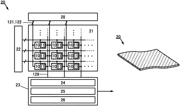
1. An imaging device comprising:
a substrate;
a pixel array; and
an adhesive layer,
wherein the substrate has flexibility,
wherein the pixel array is over a first surface of the substrate,
wherein the adhesive layer is on a second surface facing the first surface of the substrate,
wherein the pixel array comprises a light-receiving element and a light-emitting element,
wherein the light-receiving element is configured to sense infrared light,
wherein the light-receiving element comprises a first pixel electrode, a common layer, an active layer, and a common electrode,
wherein the light-emitting element is configured to emit infrared light,
wherein the light-emitting element comprises a second pixel electrode, the common layer, a light-emitting layer, and the common electrode,
wherein the active layer is over the first pixel electrode and the common layer,
wherein the active layer comprises a first organic compound,
wherein the light-emitting layer is over the second pixel electrode and the common layer,
wherein the light-emitting layer comprises a second organic compound different from the first organic compound,
wherein the common layer is over the first pixel electrode and the second pixel electrode, and
wherein the common electrode comprises a portion overlapping the first pixel electrode with the active layer therebetween and a portion overlapping with the second pixel electrode with the light-emitting layer therebetween.
|