| CPC G06V 40/1306 (2022.01) [G06F 3/0412 (2013.01); G06F 3/04166 (2019.05); G06F 3/0446 (2019.05); G06V 40/1376 (2022.01); G09G 3/3225 (2013.01); G09G 2300/0426 (2013.01); G09G 2300/0452 (2013.01); H10K 59/12 (2023.02); H10K 59/352 (2023.02); H10K 59/40 (2023.02)] | 13 Claims |

|
1. A display module comprising:
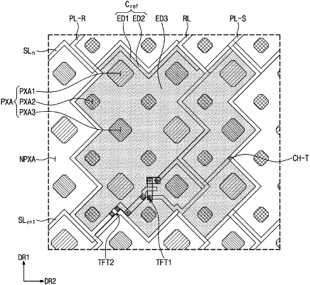
a display panel having a plurality of light emitting areas, each of the light emitting areas including a first light emitting area to emit first light having a first wavelength, a second light emitting area to emit second light having a second wavelength greater than the first wavelength, and a third light emitting area to emit third light having a third wavelength greater than the second wavelength; and
a circuit disposed on the display panel and configured to sense input signals, said circuit having a first scan line, a second scan line, a readout line, and a sensor, the sensor comprising:
a first transistor having a first input electrode to receive a power source voltage, a first output electrode connected to the readout line, and a first control electrode connected to a first node;
a second transistor having a second input electrode configured to receive an initialization voltage, a second output electrode connected to the first node, and a second control electrode connected to the second scan line;
a first electrode connected to the first scan line and spaced apart from the first light emitting areas, the second light emitting areas, and the third light emitting areas; and
a transparent electrode comprising a first portion overlapped with the first electrode to form a reference capacitor and a second portion connected to the first node,
wherein the second portion of the transparent electrode overlaps with at least two of the light emitting areas, and
wherein the first scan line and second scan line extend in a zigzag shape, the first electrode is branched from the first scan line to have the zigzag shape.
|