| CPC G06T 1/60 (2013.01) [G06F 3/0604 (2013.01); G06F 3/0631 (2013.01); G06F 3/0679 (2013.01); G06F 9/5016 (2013.01); G06T 1/20 (2013.01)] | 20 Claims |
|
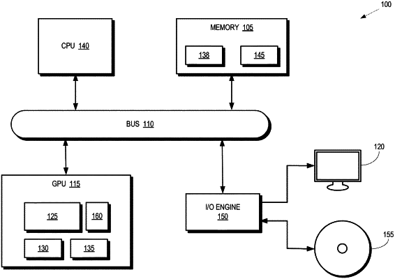
1. An apparatus comprising:
at least one processing unit; and
a resource manager circuit configured to selectively allocate a first memory portion or a second memory portion to the at least one processing unit based on application level memory access characteristics, wherein the first memory portion has a first latency that is lower than a second latency of the second memory portion.
|