| CPC G06F 30/392 (2020.01) [G06F 30/337 (2020.01); G06F 30/347 (2020.01); H01L 27/0207 (2013.01); H01L 27/0924 (2013.01); H01L 27/11807 (2013.01); G06F 30/20 (2020.01); G06F 30/373 (2020.01); G06F 30/3947 (2020.01); H01L 2027/11875 (2013.01)] | 8 Claims |

|
1. A method of fabricating a layout for an integrated circuit structure, the method comprising:
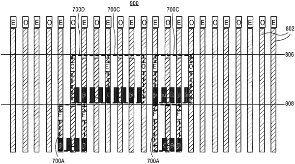
designating alternating ones of a plurality of gate lines parallel along a first direction as even (E) or odd (O) along a second direction;
selecting a location for a cell type over the plurality of gate lines;
selecting between a first version of the cell type and a second version of the cell type depending on the location, the second version structurally different than the first version, wherein the selected version of the cell type has an even (E) or odd (O) designation for interconnects at edges of the cell type along the second direction, and wherein the designation of the edges of the cell type match with the designation of individual ones of the plurality of gate lines below the interconnects.
|