| CPC G06F 3/0656 (2013.01) [G06F 3/0604 (2013.01); G06F 3/0659 (2013.01); G06F 3/0679 (2013.01)] | 14 Claims |
|
1. A data storage device, comprising:
a memory device, comprising a plurality of memory blocks, wherein the memory blocks correspond to a plurality of logical units, each logical unit corresponds to a plurality of logical addresses, the logical addresses corresponding to each logical unit are divided into a plurality of regions and each region is further divided into a plurality of sub-regions, and the sub-regions comprise one or more system data sub-regions; and
a memory controller, coupled to the memory device and configured to access the memory device,
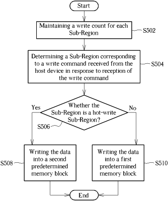
wherein the memory controller uses a first predetermined memory block as a buffer to receive data from a host device,
in response to a write command received from the host device to write data corresponding to one or more logical addresses into the memory device, the memory controller determines a sub-region corresponding to the write command according to the one or more logical addresses, determines whether the sub-region is one of the one or more system data sub-regions and accordingly determines whether to use a second predetermined memory block as another buffer to receive the data from the host device, and
wherein when the memory controller determines that the sub-region corresponding to the write command is one of the one or more system data sub-regions, the memory controller determines to use the second predetermined memory block as said another buffer and writes the data corresponding to the one or more logical addresses into the second predetermined memory block, and when the memory controller determines that the sub-region corresponding to the write command is not one of the one or more system data sub-regions, the memory controller writes the data corresponding to the one or more logical addresses into the first predetermined memory block.
|